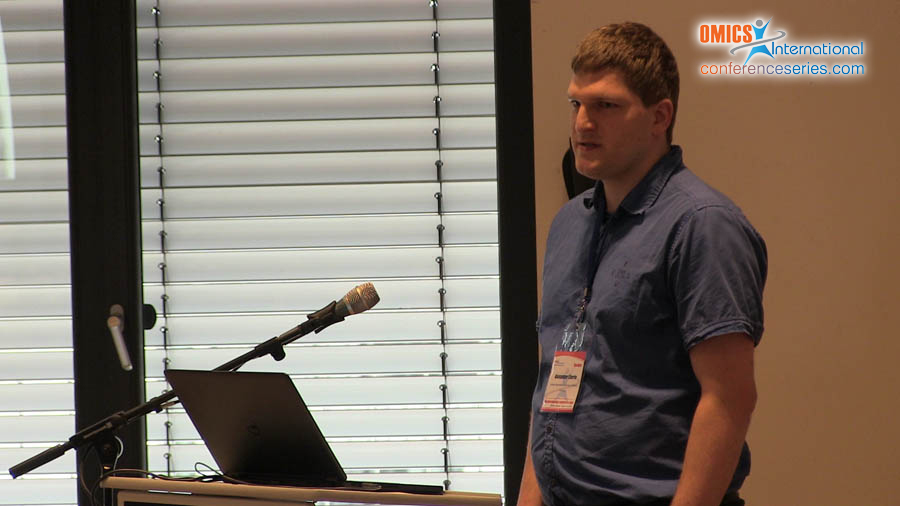
Alexander Eberle
Ludwig Maximilian University of Munich, Germany
Title: Low cost fabrication of organic semiconductor monolayer via Organic Solid-Solid Wetting Deposition (OSWD): physico-chemical basics, controllability, process capability
Biography
Biography: Alexander Eberle
Abstract
The Organic Solid-Solid Wetting Deposition (OSWD) enables the formation of monolayers made of insoluble organic semiconductors such as Pentacene, PTCDA or Quinacridone (Chem.Eur.J. 13 (2007), 7785). It’s a surface supported process that occurs on carbon substrates (graphite, graphene, nanotubes) and inorganic substrates like MoS2 and features numerous advantages compared to other monolayer growth techniques: running under ambient conditions, no requirement of expensive equipment, suitable for commercially available organic semiconductors. The OSWD is based on the physical interaction of a dispersed semiconductor-nanocrystal and a substrate. After both got in contact, under certain conditions the nanocrystal starts to wet the substrate like a liquid would do, with a gradient of the surface-free-energy as the driving force. However, a more fundamental understanding of the OSWD is necessary in order to optimize its efficiency and to further enhance the control over the nanostructure self-assembly. We used Gamma Quinacridone as a model system, an organic semiconductor extensively used in industry as a pigment. Investigations were done via Scanning Tunneling Microscopy, particle size distribution and zeta potential (ZP) analysis. Our results reveal the influence of various dispersing agents (DA) on the ability of nanocrystals to start an OSWD and on the structure of the created monolayers. The DA gives a ZP to the nanocrystals. It’s type and intensity determines the properties and the coverage rate of the monolayer.Due to our results it’s now also possible to use water as DA. These results enable a low-cost large-scale production of semiconductor-monolayers with well-defined properties.